Linear Simulation for an Amplifier
Authors: Joseph Chong, Ji Hoon Hyun, and Dr. Dong S. Ha
In this section you will learn how to design an RF amplifier working at 2.4G. Check out this workshop tutorial for more information.
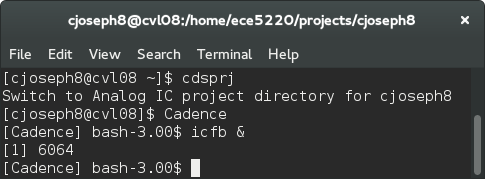
1. If you don't have Cadence Virtuoso (icfb) stated, connect to CVL and run the commands in sequence as: “cdsprj”, “Cadence”, “icfb &”.
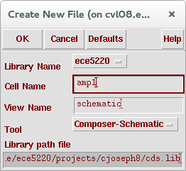
2. Create a new schematic by File->New->Cellview under icfb window. Make sure the library is the one attached to TSMC library. (For this tutorial, it is the "ece5220" library.)
3. Insert a nmos_rf transistor from tsmcN65 library. Run DC simulation to choose a desired size and DC operation point. We now choose a transistor with 2um width, 16 fingers, and bias it with VGS=0.8V and VDS=0.8V.
Recall: Insert instance by pressing key i, or click the button on the left panel, or use menu Add -> Instance.
Note: See previous tutorial for steps to create new schematic cell view and insert an instance.
See Analog IC Design Tutorial on how to perform DC analysis to a particular transistor.
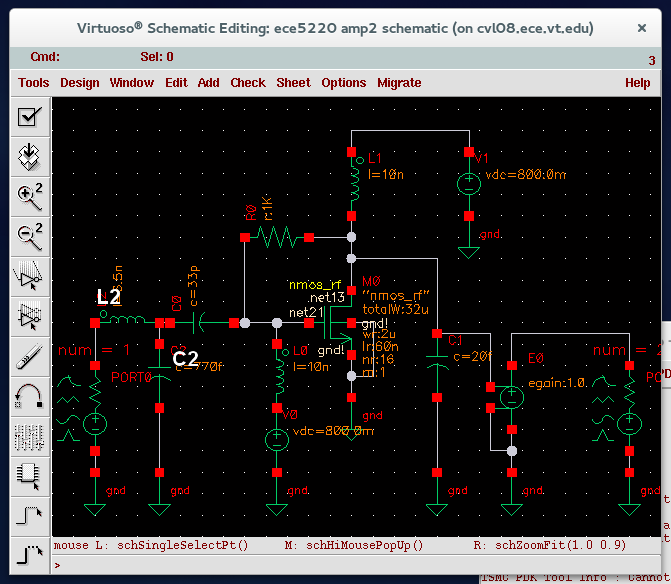
4. Our circuit topology is a common source amplifier with feedback. Create an initial schematic with DC-feeding inductors and DC-blocking capacitors as below. Since we assume the output is directly fed to another stage of transistor (CL=C1=20fF), we use a buffer to connect the signal to 50ohm port2 for simulation purpose.
Note: Select a component and right click on it, or press key q, to edit its properties. Press key w to create a wire connecting two nodes. Press ESC to cancel any previous commands.
Note: DC-feeding inductors are large inductors which acts as open circuit at high frequency. DC-blocking capacitors are large capacitors which acts as short circuit at high frequency.
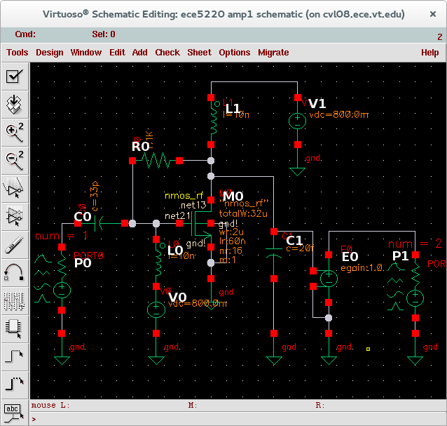
| Component | Description | Instance Library | Instance Cell | Parameter |
| V0, V1 | Voltage Source | analogLib | vdc | DC = 0.8 |
| P0 | Port | analogLib | port | Resistance = 50 / Port number = 1 |
| P1 | Port | analogLib | port | Resistance = 50 / Port number = 2 |
| L0 | Inductor | analogLib | ind | L = 10n H |
| L1 | Inductor | analogLib | ind | L = 10n H |
| C0 | Capacitor | analogLib | cap | C = 33p F |
| C1 | Capacitor | analogLib | cap | C = 20f F |
| E0 | Buffer | analogLib | VCVS | Gain = 1 |
| R0 | Resistor | analogLib | res | R = 1k |
| M0 | Transistor | tsmcN65 | nmos_rf | wr = 2u / lr = 60n / nr = 16 |
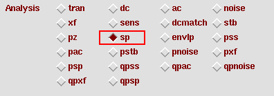
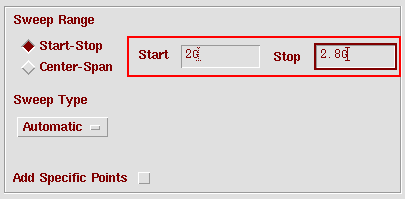
5. After finish editing, click “check & save” button to save. Start Analog Design Environment from Tools -> Analog Environment. Go to Analyses -> Choose ... and select a sp simulation from 2G to 2.8G. Run simulation by clicking the green traffic light.
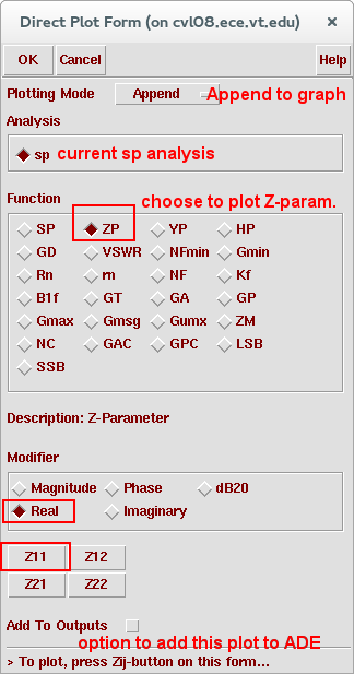
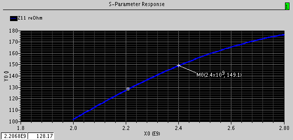
6. Go to Results->Direct Plot->Main Form and get the value of Z11 at 2.4GHz. It is the input impedance of our amplifier. Select Function as ZP, Plot Type as Rectangular, Modifier as Real, and click on the button of Z11. With the real and imaginary value of input impedance, we can design a input matching network for it.
7. Our matching network is selected as a L2 = 6.5nH series inductance and a C2=770fF shunt capacitance. Complete the schematic with them.
8. Check and save schematic. Start ADE window. Choose sp simulation. Set frequency sweep range to 2G to 2.8G. Click yes at "Do Noise" section and select output port P1 and input port P0 from schematic window. The ports will be shown as "/PORT1" and "/PORT0" or some other names according to the schematic. Click OK and click the green traffic light at ADE window to run simulation.
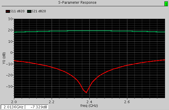
9. To plot gain and return loss performance, select Results->Direct Plot->Main Form. Select Function as SP, Plot Type as Rectangular, Modifier as dB20, and click on the button of S11, and S21. We can see that gain is around 20dB, and input return loss S11 is around -30dB indicates a good match to 50ohm.
Note: S21 and S22 will be meaningless since we have an ideal buffer.
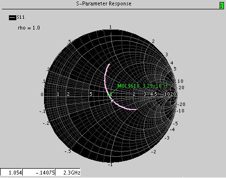
10. Back to the direct plot form, select New Win for plotting mode, change the plot type to Z-Smith, and click S11 to see input return loss shown on Smith Chart. Observe that S11 at 2.4GHz is around the middle of smith chart, indicating a good match to 50ohm.
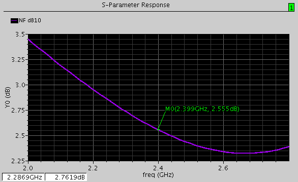
11. Back to the direct plot form, select Function as NF, Modifier as dB10, and click on the Plot button to plot noise figure performance. Noise figure at 2.4GHz is around 2.5dB.

MICS IAP Members